The world’s largest memory chip manufacturer, Samsung Electronics Co., is set to challenge the dominance of Taiwan Semiconductor Manufacturing Company (TSMC) in the foundry market by introducing an advanced three-dimensional (3D) chip packaging technology next year.
Samsung’s upcoming technology, known as Samsung Advanced Interconnection Technology (SAINT), will revolutionize the integration of memory and processors crucial for high-performance chips like artificial intelligence (AI chips), enabling significant size reduction.
Sources familiar with the matter revealed that Samsung plans to unveil three distinct technologies under the SAINT umbrella. These innovations include vertical packaging of processors such as CPU, GPU, and DRAM memory, as well as SAP S and SAP D, which involve stacking application processors and other components.
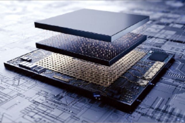
Traditionally, the current 2.5D packaging method aligns different chip types diagonally. However, Samsung is poised to introduce cutting-edge solutions like SAINT S, which have successfully completed validation tests.
Semiconductor production culminates in packaging, a crucial step that safeguards the chips from damage and facilitates interconnection. Leading players like TSMC, Samsung, and Intel Corp. are fiercely competing in advanced packaging to vertically integrate multiple chips and enhance semiconductor performance without relying on ultra-fine lithography.
The market for advanced chip packaging is projected to grow from \(44.3 billion in 2022 to \)66 billion by 2027, with 3D packaging anticipated to contribute around $15 billion to this total.
TSMC: Pioneering 3D Packaging
TSMC, a frontrunner in chip packaging technology, has been at the forefront of 2.5D packaging, a cutting-edge approach that minimizes information bottlenecks by clustering chips closely together. The company’s innovative packaging solutions cater to clients like Apple Inc. and Nvidia Corp., with substantial investments in 3D inter-chip stacking technology like SoIC.
Recently, TSMC announced a significant investment in a state-of-the-art domestic packaging facility, underscoring its commitment to advancing semiconductor packaging technology.
Samsung’s Packaging Progress
Samsung, a global leader, introduced its 2.5D package technology, H-Cube, in 2021, marking a significant milestone in chip packaging advancement. The company’s H-Cube technology enables compact stacking of logic chips or high-bandwidth memory on a silicon interposer, enhancing performance and efficiency.
In a bid to bolster AI chip performance for data centers and devices with on-device AI capabilities, Samsung is leveraging its SAINT technology, aiming to provide tailored packaging services encompassing chip manufacturing, packaging, and testing.