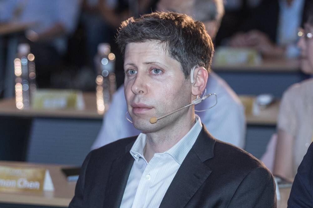
Sam Altman, the Chief Executive Officer of OpenAI, is reportedly seeking funding to establish semiconductor production facilities dedicated to manufacturing processors for artificial intelligence (AI) applications, according to a report by Bloomberg. Altman envisions a future where AI technologies will be so prevalent that they will require their own specialized semiconductor supply chain. This move would position OpenAI in direct competition with established players like Intel, TSMC, and Samsung Foundry.
At present, OpenAI relies on Nvidia’s A100 and H100 GPUs to drive its widely-used Chat GPT service. However, recent reports indicate that the organization is actively exploring the development of its own AI-focused processors. This strategic shift aligns with the trend seen among major hyperscalers such as Amazon Web Services, Google, and Microsoft, who are opting to design custom processors in addition to utilizing off-the-shelf solutions.
In a departure from traditional strategies, Altman’s vision extends beyond creating standalone AI chips. Described as a ‘network of AI chip factories’ by Bloomberg, this ambitious initiative involves engaging with potential investors like G42 and SoftBank Group. The main goal is to tackle the current and anticipated scarcity of AI-specific semiconductor chips. Altman predicts that traditional foundries like TSMC, Samsung Foundry, and Intel Foundry Services may face challenges in meeting the increasing demand for AI-focused chips in the future.
The financial scale and operational intricacy of this project are substantial. Initial discussions with G42 centered around securing funding ranging from \(8 billion to \)10 billion. The detailed scope of the project and the list of partners are still in the early stages, highlighting the significant investments and lengthy timelines needed to establish a network of such manufacturing facilities. It is unclear whether Altman plans to acquire an existing foundry for AI chip production or build a new network of fabs tailored to the needs of OpenAI and its potential partners.
The development of a 2nm or 3nm class process technology requires investments in the billions of dollars, with costs increasing as fabrication nodes shrink. Currently, constructing an advanced fab capable of mass-producing chips on a 3nm or 2nm-class node can cost around \(30 billion. Additionally, the expenses related to fab operations are rising, with a single Low-NA EUV lithography tool priced at approximately \)200 million and estimates suggesting that a High-NA lithography machine could cost between \(300 million to \)400 million. Ensuring a cutting-edge fab is future-proofed for AI and HPC applications involves deploying multiple Low-NA and High-NA machines.
The ability of Altman to secure tens or even hundreds of billions for fab construction, ensure their continuous operation, and supervise the production of state-of-the-art chips is a matter that only time will reveal. Nonetheless, it is evident that his efforts have the potential to disrupt the current landscape of the foundry market.


