
Multifunctional computer chips have advanced to incorporate integrated sensors, processors, memory, and other specialized components, expanding their capabilities. However, with this growth in chip complexity comes an increase in the time needed to transfer information between these functional elements.
According to Sang-Hoon Bae, an assistant professor of mechanical engineering and materials science at the McKelvey School of Engineering at Washington University in St. Louis, this evolution can be likened to constructing a house. As you expand both horizontally and vertically to accommodate more functions and specialized activities, the necessity for moving or communicating between different areas also escalates.
To tackle this challenge, Bae and an international team of researchers, including experts from institutions such as the Massachusetts Institute of Technology, Yonsei University, Inha University, Georgia Institute of Technology, and the University of Notre Dame, have showcased the monolithic 3D integration of layered 2D material into innovative processing hardware for artificial intelligence (AI) computing. Their innovative approach aims not only to offer a material-level solution for fully integrating numerous functions into a compact electronic chip but also to pave the way for advanced AI computing capabilities. This groundbreaking research was recently featured in Nature Materials, where it was highlighted as a front cover article.
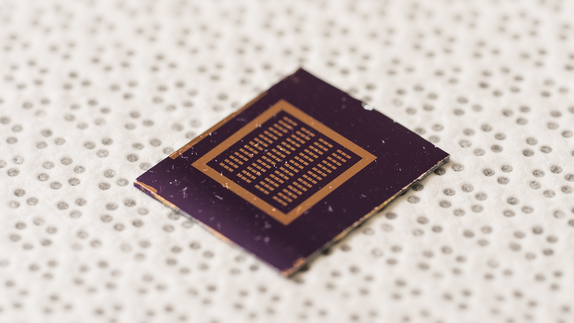
The monolithic 3D-integrated chip developed by the team presents several advantages over conventional laterally integrated computer chips. By incorporating six atomically thin 2D layers, each serving a specific function, the chip achieves notable reductions in processing time, power consumption, latency, and footprint. This efficiency is made possible by densely packing the processing layers to ensure robust interlayer connectivity. Consequently, the hardware delivers unparalleled efficiency and performance in AI computing tasks.
This breakthrough not only provides a fresh approach to integrating electronics but also heralds a new era of multifunctional computing hardware. With its core emphasis on ultimate parallelism, this technology has the potential to significantly enhance the capabilities of AI systems, enabling them to tackle complex tasks swiftly and accurately.
Bae envisions that monolithic 3D integration could revolutionize the electronics and computing industry by enabling the development of more compact, powerful, and energy-efficient devices. Leveraging atomically thin 2D materials, the team aims to refine this technology further to eventually integrate all functional layers onto a single chip.
Moreover, these devices exhibit enhanced flexibility and functionality, making them suitable for a wide array of applications. From autonomous vehicles to medical diagnostics and data centers, the possibilities presented by this monolithic 3D integration technology are vast. For instance, in-sensor computing merges sensor and computer functionalities into a single device, eliminating the need for data transfer between a sensor and a computer. This approach accelerates processing, reduces energy consumption, and enhances security by computing data directly at the source.
For more details, refer to the original publication by Kang J-H, Shin H, Kim KS, Song M-K, Lee D, Meng Y, Choi C, Suh JM, Kim BJ, Kim H, Hoang AT, Park B-I, Zhou G, Sundaram S, Vuong P, Shin J, Choe J, Xu Z, Younas R, Kim JS, Han S, Lee S, Kim SO, Kang B, Seo S, Ahn H, Seo S, Reidy K, Park E, Mun S, Park M-C, Lee S, Kim H-J, Kum HS, Lin P, Hinkle C, Ougazzaden A, Ahn J-H, Kim J, and Bae S-H, titled “Monolithic 3D integration of 2D materials-based electronics towards ultimate edge computing solutions,” published in Nature Materials on Nov. 27, 2023. [DOI: https://doi.org/10.1038/s41563-023-01704-z]
This research was made possible with the support of various institutions, including Washington University in St. Louis, the Korea Institute of Science and Technology, the National Research Foundation of Korea, the National Science Foundation, and SUPREME, part of the JUMP 2.0 program sponsored by DARPA.
This article was originally published on the McKelvey School of Engineering website.